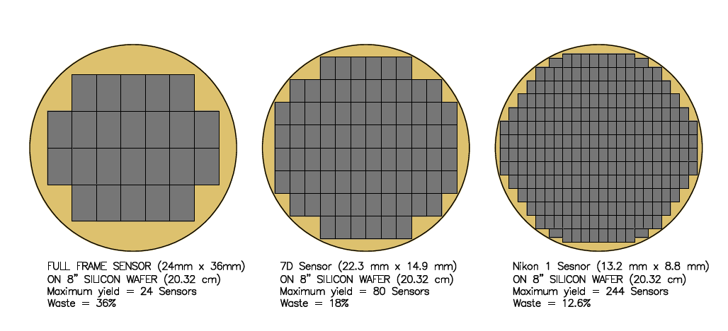
MichaelT posted an answerMichaelT posted an answer to the question "What limits the size of digital imaging sensors?" which included this illustration of why increasing the size of the sensor leads to an increase of wasted silicon wafer area:

However, the "maximum yield" calculation seems wrong here, and as an implication of that, the waste figure as well. There is a lot of silicon that isn't getting used particularly in the "full frame sensor" illustration in the above image.
What is there to stop using the area surrounding the set of larger sensors for smaller ones? Is it just a matter of the process that is currently used, or is there something inherent to the making of digital imaging sensors that makes such a (multiple-sensor-sizes) process impractical? Or is the illustration overly simplified (and thus the numbers misleading), and that's what manufacturers already do?
